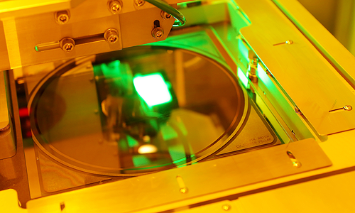
Enliten offers a Wafer Level CSP low cost solution that enables direct connectivity at the substrate or board level. To help provide this service we are equipped with latest state-of-the art Laser Mark, Laser Groove, Camtek & Rudolph Wafer 2D/3D inspection station and high speed Muhlbauer Die Sorter. We offer a full turnkey solution for Wafer Level CSP from WAFER BUMPING, PACKAGING, TEST SOLUTION (probing) and full wafer map integration to handle die size from 0.2 sq.mm to 36 sq.mm.
 Package Configurations (PDF).pdf