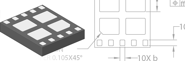
Enliten’s MIS Package uses a Molded Interconnect Substrate (MIS) technology to create a package with an overall thickness of only 0.33 mm or lower. This technology allows for high IO counts in a small form factor because of the Cu trace routing capability and is perfect for devices requiring a high performance solution with low noise or high frequency. Applications for this package include consumer, communications, data storage, computing and automotive.
 Package Configurations (PDF).pdf